 電子發燒友App


 創作
創作 發文章
發文章 發帖
發帖  提問
提問  發資料
發資料 發視頻
發視頻資料介紹
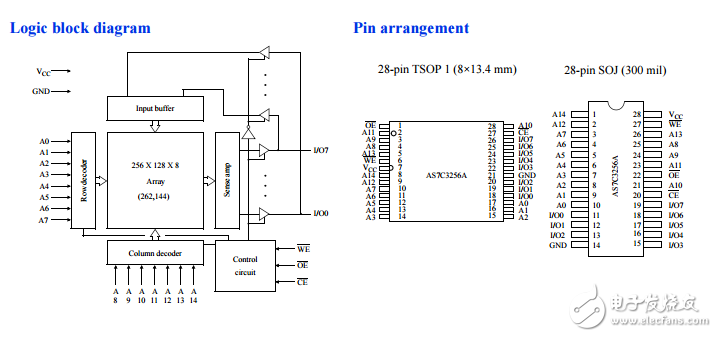
The AS7C3256A is a 3.3V high-performance CMOS 262,144-bit Static Random-Access Memory (SRAM) device organized as 32,768 words × 8 bits. It is designed for memory applications requiring fast data access at low voltage, including PentiumTM, PowerPCTM, and portable computing. Alliance’s advanced circuit design and process techniques permit 3.3V operation without sacrificing performance or operating margins. The device enters standby mode when CE is high. CMOS standby mode consumes 7.2 mW. Normal operation offers 75% power reduction after initial access, resulting in significant power savings during CPU idle, suspend, and stretch mode. Equal address access and cycle times (tAA, tRC, tWC) of 10/12/15/20 ns with output enable access times (tOE) of 5, 6, 7, 8 ns are ideal for high-performance applications. The chip enable (CE) input permits easy memory expansion with multiple-bank memory organizations. A write cycle is accomplished by asserting chip enable (CE) and write enable (WE) LOW. Data on the input pins I/O0-I/O7 is written on the rising edge of WE (write cycle 1) or CE (write cycle 2)。 To avoid bus contention, external devices should drive I/O pins only after outputs have been disabled with output enable (OE) or write enable (WE)。 A read cycle is accomplished by asserting chip enable (CE) and output enable (OE) LOW, with write enable (WE) high. The chip drives I/O pins with the data word referenced by the input address. When chip enable or output enable is high, or write enable is low, output drivers stay in high-impedance mode. All chip inputs and outputs are TTL-compatible. Operation is from a single 3.3 ±0.3V supply. The AS7C3256A is packaged in high volume industry standard packages.
- 5V輸入、3.3V/1.3A輸出、I/O電源驅動微處理器參考設計
- LT1585-3.3演示電路-3.3V、4.6A穩壓器(4.75-7V至3.3V@4.6A)
- LT1584-3.3演示電路-3.3V、7A線性調節器(4.75-7V至3.3V@7A)
- 3.3 V CMOS SRAM 64K×16,AS7C31026B數據手冊 2次下載
- 引腳兼容as7c4096 CMOS SRAM數據 3次下載
- 8標準32K的SRAM,U62256a數據資料下載 9次下載
- as7c316096b 1 2048k x 8位高速CMOS SRAM 2次下載
- AS7C31024B,3.3V的CMOS 128K的×8的SRAM 2次下載
- AS7C34098A,3.3伏的CMOS SRAM的256K×16 4次下載
- cy7c1347g 4兆位(128K的×36)流水線同步SRAM 6次下載
- cy7c199cn 256的速率(32 K×8)靜態RAM 9次下載
- 確保光學隔離3.3V I2C總線的數據完整性 0次下載
- XAPP520將符合2.5V和3.3V I/O標準的7系列FPGA高性能I/O Bank進行連接 75次下載
- AS7C256 pdf(5V/3.3V 32K X 8 CMOS SRAM)
- 24C32 CMOS I²C 2-WIRE BUS
- 如何將5V輸出安全轉換為3.3V輸入 5906次閱讀
- 3.3V穩壓電源設計 6797次閱讀
- 9種實用的將3.3V輸出連接到5V輸入的方法! 3983次閱讀
- 高效DC/DC轉換器從3.3V背板提供兩個15A輸出 1313次閱讀
- 如何將5V系統的輸出接到3.3V系統的輸入上呢 3940次閱讀
- 解析3.3V與5V雙向電平轉換電路的工作狀態 1.5w次閱讀
- 電源中的+12V/+5V/+3.3V都給哪些硬件供電? 4w次閱讀
- 3.3V供電的RS485接口滿足遠距離通訊要求 3.1w次閱讀
- 3.3v穩壓電路電容作用 3.3v穩壓電路典型電路圖及分析 4w次閱讀
- 了解I-9K與I-97K系列I/O擴充模塊性能與適用范圍 4395次閱讀
- 新產品上市:I-9K與I-97K系列 I/O擴充模塊 4197次閱讀
- 5V轉3.3V如何設計方案? 4121次閱讀
- 12v轉3.3v電路圖大全(五款12v轉3.3v電路原理圖詳解) 8.7w次閱讀
- 信號鏈基礎知識:工業市場過渡到3.3V CAN收發器 3943次閱讀
- 隔離式3.3V轉5V轉換器的分立設計 4249次閱讀

 上傳資料賺積分
下載排行
本周
- 1AN-1267: 使用ADSP-CM408F ADC控制器的電機控制反饋采樣時序
- 1.41MB | 5次下載 | 免費
- 2AN158 GD32VW553 Wi-Fi開發指南
- 1.51MB | 2次下載 | 免費
- 3嵌入式軟件開發符合ISO 26262 功能安全標準
- 1.61 MB | 1次下載 | 免費
- 4AN148 GD32VW553射頻硬件開發指南
- 2.07MB | 1次下載 | 免費
- 5AN-793: iCoupler隔離產品的ESD/閂鎖考慮因素
- 1.01MB | 次下載 | 免費
- 6AN-718: ADuC7020評估板參考指南
- 413.19KB | 次下載 | 免費
- 7EE-205:將代碼從ADSP-TS101S TigerSHARC處理器移植到ADSP-TS201S TigerSHARC處理器的注意事項
- 351.6KB | 次下載 | 免費
- 8HSW-TTY6754 二鍵觸摸感應IC_V1
- 1.15 MB | 次下載 | 免費
本月
- 1ADI高性能電源管理解決方案
- 2.43 MB | 451次下載 | 免費
- 2免費開源CC3D飛控資料(電路圖&PCB源文件、BOM、
- 5.67 MB | 138次下載 | 1 積分
- 3基于STM32單片機智能手環心率計步器體溫顯示設計
- 0.10 MB | 130次下載 | 免費
- 4使用單片機實現七人表決器的程序和仿真資料免費下載
- 2.96 MB | 44次下載 | 免費
- 5美的電磁爐維修手冊大全
- 1.56 MB | 24次下載 | 5 積分
- 6如何正確測試電源的紋波
- 0.36 MB | 19次下載 | 免費
- 7感應筆電路圖
- 0.06 MB | 10次下載 | 免費
- 8萬用表UT58A原理圖
- 0.09 MB | 9次下載 | 5 積分
總榜
- 1matlab軟件下載入口
- 未知 | 935121次下載 | 10 積分
- 2開源硬件-PMP21529.1-4 開關降壓/升壓雙向直流/直流轉換器 PCB layout 設計
- 1.48MB | 420062次下載 | 10 積分
- 3Altium DXP2002下載入口
- 未知 | 233088次下載 | 10 積分
- 4電路仿真軟件multisim 10.0免費下載
- 340992 | 191367次下載 | 10 積分
- 5十天學會AVR單片機與C語言視頻教程 下載
- 158M | 183335次下載 | 10 積分
- 6labview8.5下載
- 未知 | 81581次下載 | 10 積分
- 7Keil工具MDK-Arm免費下載
- 0.02 MB | 73810次下載 | 10 積分
- 8LabVIEW 8.6下載
- 未知 | 65988次下載 | 10 積分


 工商網監
工商網監
評論