 基于PM8805封裝系統級芯片的智能以太網供電解決方案
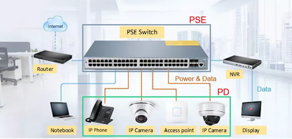
ST公司的PM8805是封裝系統級芯片,用于以太網供電(PoE)供電器件(PD),可用功率水平高達99.9W.器件嵌入兩個有源橋及其驅動電路與驅動高邊MOSFET,熱插拔MOSFET和兼容IEEE 802.3bt的電池泵.PM8805能進行物理層分類,提供有成效的PSE認證身份證明標識,可確認出4對PSE,信息由專用的Tx信號矩陣來提供。器件由以太網電纜的電源或由外接電源如墻上適配器。 PM8805集成了100V N溝MOSFET,總通路電阻為0.2Ω,100V 0.1Ω高邊熱插拔MOSFET,PoE-PD單識別標志接口和IEEE 802.3bt/at/af兼容,支持對PoE應用,支持12V輔助源,智能工作模式,熱關斷保護,主要用在大功率無線數據系統,安全照相機,接入點,公共信息顯示以PoE照明系統。本文介紹了PM8805主要特性,內部框圖,應用電路,以及大功率PoE PD/5 V高達20A有源箝位正向評估板STEVAL-POE003V1主要特性別,電路圖和材料清單以及PCB設計圖與裝配圖。
The PM8805 is a system-in-package for smartpower supply of Power over Ethernet (PoE)Powered Devices (PD) and it is applicable forpower level up to 99.9 W.
It embeds: two active bridges and their drivingcircuitry, a charge pump to drive the high-sideMOSFETs, the hot swap MOSFET and theinterface compliant with IEEE 802.3bt.
The device performs the physical layerclassification, providing the indication ofsuccessful PSE type identification. A 4-pair PSEis identified and the information is available by adedicated matrix of Tx signals.
The device works with power either from theEthernet cable or from an external power sourcesuch as a wall adapter, with possible prevalenceof the auxiliary source with respect to the PoE.
The PM8805 is suitable to build the interfacesection of PoE switch mode power supplies targeting the highest conversion efficiency. Itprovides a PGD signal that can be used to enablea PWM controller, a DC-DC converter or an LEDdriver.
The PM8805 integrates a dual MOSFET bridge and a PD-PoE single-signature interface,specifically designed to support high power, 4-pair (4P) applications, as being specified in the new IEEE802.3bt standard, but also capable of working with high efficiency, 2P applications.
Typically, after the data transformer a diode bridge is used to set a defined polarity to the input voltage since such polarity on the Ethernet cable may vary.
Considering the maximum power levels defined by the IEEE802.3-2015 standard (25 W fora Type2 PD) the diode bridges power losses may still be acceptable, but with new powerhungry applications like UPOE, with more than 50 W at PD end, the power losses of astandard diode bridge become too high.
The same consideration is valid for standard applications that need to squeeze the maximum available power from the PSE. For example, comparing a diode bridge with Vd= 0.8 V with bridged 100 mΩ Ron MOSFETs, the gain at 0.5 A, 50 V is about 0.75 W out of 25W, i.e. about 3% on overall efficiency.
PM8805主要特性:
? Dual active bridge, hot swap MOSFETandPoE-PD interface in a system-in-package
? 100 V N-ch MOSFETs with 0.2 Ω total pathresistance for each active bridge.
? 100 V, 0.1 Ω high-side N-ch hot swap MOSFET
? PoE-PD single-signature interface compliantwith IEEE 802.3bt / at / af
? Supports 4-pair PoE applications
? Supports 12 V auxiliary sources
? Identifies which kind of PSE (standard orlegacy) is connected with and provides successful IEEE802.3bt/at/af classificationindication as a combination of the T0, T1 andT2 signals (open drain)
? Smart operational modes
? Programmable classification current with3.3 ms delay.
? Optional Autoclass feature
? Advanced energy-saving MPS timings
? Two-step hot swap current protection: DC with1 ms delay and short-circuit with 10 us delay.
? Controlled pre-charge of the output capacitor
? PGD signal (open drain) to enable an externalPWM controller.
? Thermal shutdown protection
PM8805應用:
? High power wireless data systems
? Security cameras
? Access points
? Public information displays
? PoE lighting systems
圖1.PM8805內部框圖
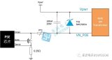
圖2.采用PM8805輸入級的PD簡化應用電路圖
圖3.采用PM8805和DC/DC前CM濾波器的PD簡化通用電路圖

圖4.簡化的前輔助連接器電路圖
圖5.簡化的后輔助連接器電路圖
圖6.PM8805應用案例布局圖
大功率PoE PD/5 V高達20A有源箝位正向評估板STEVAL-POE003V1
This evaluation board implements a PoE Class 8 converter that is compliant with the IEEE802.3bt standard. The PoE interface is based on the PM8805 PoE-PD interface and a DC-DC forward active clamp converter based on the PM8804 controller.
The PM8805 system on package device embeds two active bridges and anIEEE802.3bt compliant Powered Device (PD) interface. It can be used in all mediumto-high power 2P and 4P high efficiency PoE and PoE+ applications.
The PM8804 PWM controller integrates all the circuitry required for a smart andefficient 48 V converter, including a programmable oscillator for the switchingfrequency, adjustable slope compensation, dual complementary low-side drivers withprogrammable dead time, programmable soft start, soft turn off and a programmablecurrent sense blanking time.The device targets high efficiency conversion over a wide load range.
The STEVAL-POE003V1consists of a POE interface compliant with the last standard IEEE802.3bt, created withthe PM8805 interface and a forward active clamp DC-DC converter that receives a DC voltage from POEinterface.
PM8805 device integrates two N-channel MOSFET bridges, one for every 2-pair of the POE interface, and anhotswap MOSFET placed in series with the outputs of two bridges. The following figure shows the efficiency of the single forward converter, and the overall efficiency that alsoincludes the power losses of the POE interface.
評估板STEVAL-POE003V1主要特性:
? Features of PM8805
– System in package integrating a double active bridge, a hot-swap MOSFETand a PoE-PD interface
– PoE-PD single-signature interface compliant with IEEE 802.3bt
– Detection and support of high power 4-pair applications
– 100 V N-Ch MOSFETs with 0.2 Ω total path resistance for each activebridge
– Identifies which kind of PSE (standard or legacy) it is connected to andprovides successful IEEE802.3 af / at / bt classification indication as acombination of the T0, T1 and T2 signals (open drain)
– VFQFPN43 8x8 mm with 6 exposed pads
? Features of PM8804
– PWM peak current mode controller
– Input operating voltage up to 75 V
– Internal high voltage start up regulator with 20 mA capability
– Programmable fixed frequency up to 1 Mhz
– Soft start up with settable time
– Soft turn off (optionally disabled)
– Dual 1Apk, low side complementary gate drivers
– GATE2 optionally turned off for reduced consumption
– 80% maximum duty cycle with internal slope compensation
– VFQFPN 3.0x3.0x1.0 16L 0.5 mm pitch
? WEEE compliant
? RoHS compliant
圖7.評估板STEVAL-POE003V1外形圖
評估板STEVAL-POE003V1主要指標:
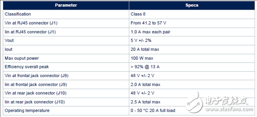
圖8.評估板STEVAL-POE003V1 PCB頂層裝配圖
圖9.評估板STEVAL-POE003V1 PCB底層裝配圖
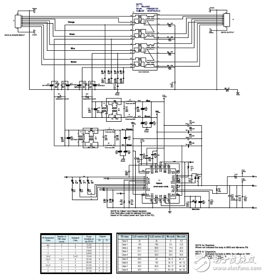
圖10.評估板STEVAL-POE003V1電路圖(1)
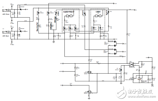
圖11.評估板STEVAL-POE003V1電路圖(2)
圖12.評估板STEVAL-POE003V1電路圖(3)
評估板STEVAL-POE003V1材料清單:

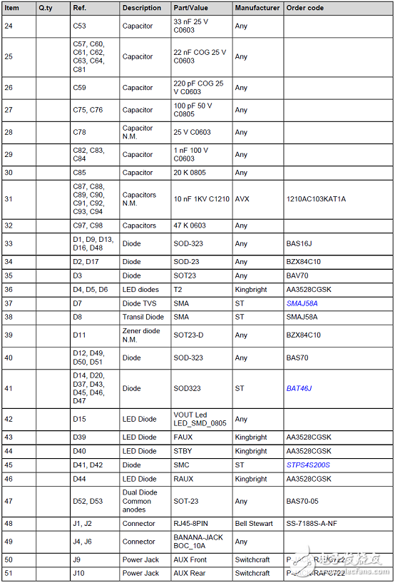


圖13.評估板STEVAL-POE003V1 PCB設計圖(1):層1頂層

圖14.評估板STEVAL-POE003V1 PCB設計圖(2):層2
圖15.評估板STEVAL-POE003V1 PCB設計圖(3):層3

圖16.評估板STEVAL-POE003V1 PCB設計圖(4):層4
圖17.評估板STEVAL-POE003V1 PCB設計圖(5):層5
圖18.評估板STEVAL-POE003V1 PCB設計圖(6):層6
-
以太網
+關注
關注
40文章
5460瀏覽量
172724 -
封裝系統
+關注
關注
0文章
4瀏覽量
7882
發布評論請先 登錄
相關推薦
POE以太網供電浪涌防護
以太網供電 (PoE)/LAN 防護解決方案概述
以太網供電完全自主的四端口供電設備解決方案
以太網怎么為工業市場供電?
【亞信電子】任天堂Switch - 亞信USB以太網芯片解決方案演示視頻
如何利用以太網為工業市場供電
關于高效的以太網供電解決方案的應用介紹

Linux以太網解決方案的介紹
基于新一代IEEE 802.3bt以太網供電標準系統的解決方案

POE以太網供電浪涌保護方案


 工商網監
工商網監
評論